Research / Liquid Cells for In-situ Electron Microscopy
Another direction of our research is the application of 2D materials for atomic resolution imaging of chemical processes in liquid environment. Transmission electron microscopy (TEM) is a powerful tool for imaging and characterising materials at the nanoscale, but the high vacuum inside the microscope column usually limits the nature of the observable samples. While the majority of application-relevant chemical processes take place in liquids or gases, studying them in TEM presents a challenge.
Liquid cells employ two electron transparent but impermeable membranes to contain a liquid sample, preventing it from evaporating under the high vacuum environment of the electron microscope and enabling dynamic imaging of liquid samples. However, the thickness of the windows and the liquid layer generates increased electron scattering, limiting the ultimate resolution. By replacing commercially available silicon nitride windows (20 – 50 nm thick) with graphene windows, we can reduce the window thickness to below 1nm, dramatically reducing electron scattering and therefore improving imaging ability.

Cross-section of a double liquid cell structure. Two hBN spacer layers, each tens of nm thick, with a molybdenum disulfide (MoS2) monolayer sandwiched between them (central layer, coloured purple in the figure). Both hBN spacers contain voids pre-patterned using electron-beam lithography and reactive-ion etching. Liquid samples are trapped inside the voids using few-layer graphene (FLG) on the top and bottom of the stack (coloured in green). The atomically flat hBN crystals form a hermetic seal with graphene and MoS2. Inset top right: HAADF-STEM image. The probe is focused on the submerged MoS2 layer so that the Mo lattice and Pt adatoms are clearly visible. Inset bottom right: A single Pt adatom trajectory from a 134 s video in the graphene double liquid cell
Our engineered graphene liquid cell (EGLC) designs are based on van der Waals heterostructures, with a patterned spacer layer of 2D material defining liquid pockets which are then sealed using graphene.
The strong interaction between the 2 atomically flat surfaces generates hermetically sealed individual microwells, with a tuneable thickness down to < 10 nm which is consistent across each cell. The favourable imaging conditions have allowed us to demonstrate nanometre resolution elemental mapping, and atomic resolution ADF STEM imaging.
Our heterostructure based EGLC also allows for more complicated experiments.
For example, by adding a beam sensitive separation layer between two separate EGLC pockets, we can induce local mixing of two precursor solutions directly under the field of view of the microscope by controlled fracturing, allowing us to capture the very earliest stages of solution phase chemical reactions. This was applied to study nonclassical nucleation of calcium carbonate at the nanometre scale.
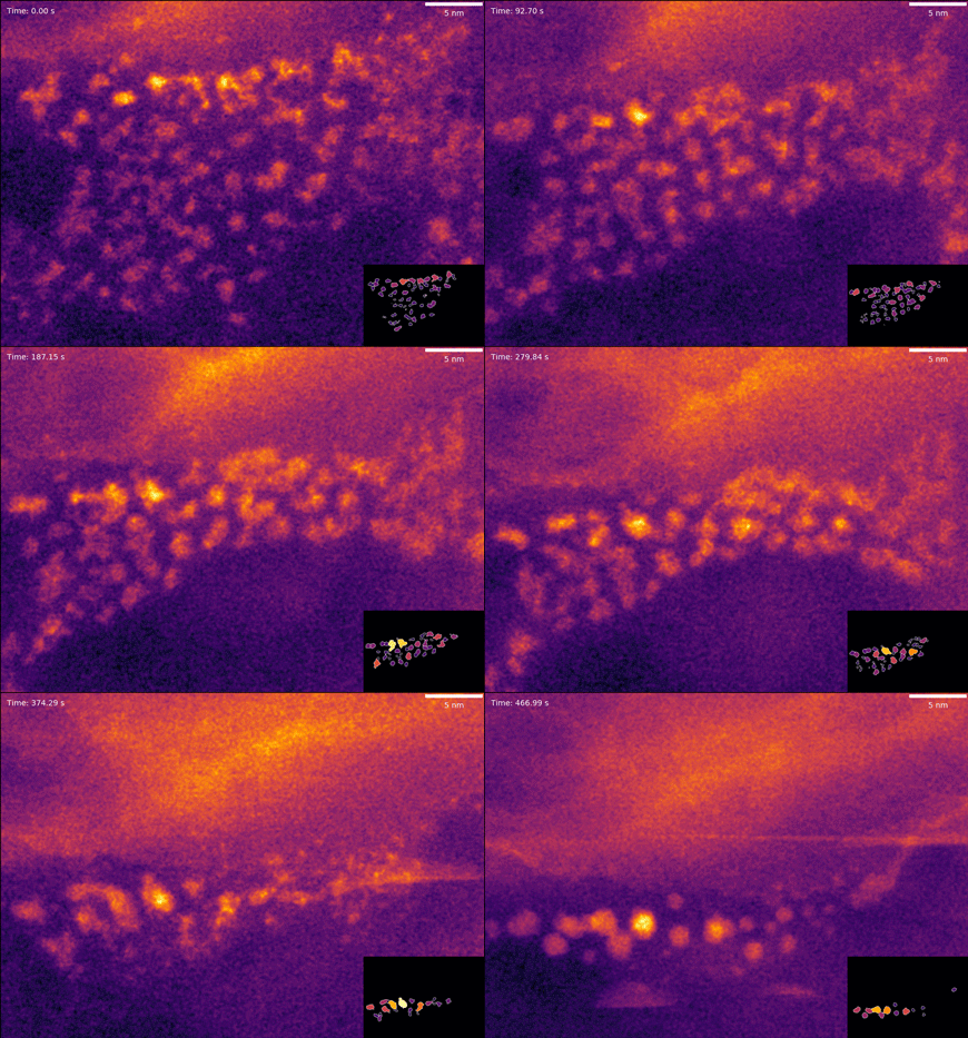
Schematic of a 2D-mixing cell. Two pockets of separate liquids (represented by red and green spheres) formed in microwells in a hBN flake and sealed with graphene windows are separated by an MoS2 monolayer. The separation layer can be punctured using the beam, allowing the two solutions to mix and react in the direct field of view of the microscope. Nonclassical nucleation of amorphous calcium carbonate from upon mixing 2 precursors. Dense liquid phases formed upon initial mixing spontaneously dehydrate and coalesce to form spherical particles.


Nonclassical nucleation of amorphous calcium carbonate from upon mixing 2 precursors. Dense liquid phases formed upon initial mixing spontaneously dehydrate and coalesce to form spherical particles.
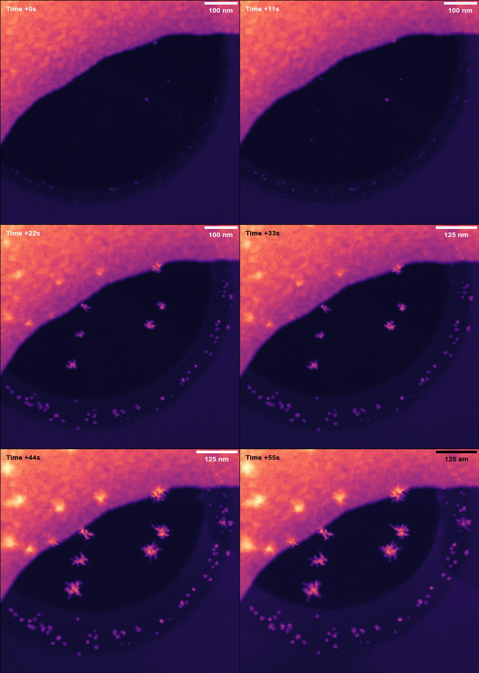
Beam induced growth of dendritic gold particles from solution in acetone within an EGLC.
