top of page

Research

​

Van der Waals heterostructures, assembled from 2D materials, offer unprecedented opportunities for the design and fabrication of nanostructures with tailored properties and novel physics. Our research is focused on physics and chemistry of quantum solid state systems, which emerge in heterostructures build from atomically thin 2D crystals. It can be broadly separated in two areas: studies of electronic and optical properties of van der Waals heterostructures (for instance, twistronics), and observation of chemical reactions in liquids with atomic resolution electron microscopy. An essential component shared by both research directions is the novel nanofabrication methods we develop for proof-of-principle prototyping and small-scale manufacturing aiming to advance quantum technologies, low power electronics, and catalysis.

​


Advanced Nanofabrication

​

Advanced Nanofab

Our group’s research focuses on developing novel advance fabrication techniques to produce high quality 2D materials heterostructures (2DMH), assembled layer-by-layer with ultra-sharp and ultra-clean interfaces. For this purpose, we have developed a pioneering UHV-Press system, allowing the fabrication and characterisation of 2DMH in ultra-high vacuum environments. To convert these 2DMH into devices, we count with state-of-the-art equipment in an   ISO class 5 & 6 cleanroom over two floors at the NGI.

​

To date, the 2D materials family has thousands of crystals with diverse optoelectronic properties, including wide and narrow-band semiconductors, metals and semimetals, superconductors, ferromagnets and antiferromagnets. The most famous representatives include the semi-metallic graphene, the wide band-gap insulator hBN, and the semiconducting transition metal dichalcogenides (TMDs), which gained scientific momentum due to their exciting properties and exceptional environmental stability in monolayer form. However, 2D crystals are not only interesting in isolated form. Much of the excitement of 2D materials stems from our ability to combine them in any desired sequence layer-by-layer and with controlled twisting angles to produce 2D material heterostructures (2DMH) with atomically sharp and clean interfaces. Unlike conventional crystal growth, their fabrication is not restrained by lattice matching or interfacial chemistry and therefore offers a versatile platform for creating unique quantum and optoelectronic metamaterials with properties tailored for particular applications.

Despite the great academic interest and high application potential, the field has been held back by the extreme cleanliness necessary to reach the limit where 2DMH display quantum properties. All existing techniques rely on polymeric matrices to produce the stacks, and cannot avoid the presence of airborne hydrocarbon molecules on the surface of the exfoliated crystals. When trapped between layers, these molecules coalesce into bubbles and distort the properties of the 2DMH. Furthermore, many 2D materials are very sensitive to air, degrading fast when exposed to the atmosphere. Thus, they require special fabrication procedures performed in controlled environments such as Ar or vacuum, in order to preserve the intrinsic properties of the crystals.

​

​

​

​

​

​

​

​

​

​

​

​

​

​

​

​

​

​

​


​

2D materials heterostructures (2DMH) are fabricated stacking atomically thin layers of materials on top of each other, in a similar fashion as LEGO blocks. [1]

Frabrication.jpg

​

One of our main directions is development of a unique ultra-high vacuum press (UHV-Press) system, that allows stacking 2D crystals at pressures down to , comparable with the state-of-the-art of other fabrication techniques such as molecular beam epitaxy (MBE). 

​

JIL3087-800x450.jpg

Ultra-high vacuum press (UHV-Press) system developed to provide the cleanest atmosphere possible for the fabrication of 2DMH.

​

Together with this, a ground-breaking heterostructure fabrication procedure has been developed by the team substituting the ubiquitous polymeric matrices by completely inorganic, UHV-compatible technology. The combination of these two technologies ensures the complete removal of hydrocarbon contamination, and eliminates the oxygen- and water-induced degradation of sensitive 2D materials. Removing this obstacles bring us much closer to achieving electronic-grade 2D heterostructure technology, the key for the development of novel nanoscale applications based on 2D materials in quantum technologies, low-power (opto)electronics.

[1]    Geim, A.K. & Grigorieva, I.V. Van der Waals heterostructures. Nature, 499, 419-425 (2013).

​

Twistronics

Twistronics

Twistronics is an emerging field that became available once the ability to precisely control of the relative twist angle between adjacent 2D crystals was developed. Introducing twist between 2D crystals with similar lattice constants gives rise to moiré superlattices - a periodic variation of a local atomic registry, which in turn causes modulation of interlayer hybridisation, symmetry and strain, unlocking a new way to tune the electronic and optical properties of the 2DMH.

​

Our group recently demonstrated that atomic lattices of Transition Metal Dichalcogenides undergo substantial reconstruction for small enough twist angles (θ<2°). As a result, instead of gradually changing atomic displacement between the lattices, perfectly stacked bilayer regions (or domains) form, which possess lower adhesion energy between the layers compared to that of two twisted lattices. Such lattice adjustment is accompanied by the strain which accumulates within narrow domain boundaries, resulting in a periodic domain network separated by a network of dislocations.

​

Unlike graphene, stacking two monolayer of TMDs with parallel and anti-parallel orientation of the unit cells (without twist) produces different polytypes, known as 3R and 2H for bulk TMDs, respectively. Introducing a small twist angle leads to the formation of the domain network which we have recently described using transmission electron microscopy (TEM) and Conductive AFM in our paper in Nature Nanotechnology [1]. For the twisted 3R-type heterostructures, a network of triangular domains form corresponding to commensurate MX’ and XM’ stacking (i.e. M: metal atom; X: chalcogen atom). On the other hand, for twisted 2H-type structures a kagome-like patterns emerges, tessellated with MM’ and 2H stacking. This striking difference in the network layout is due to the energy balance between the constituent stacking: the twisted 3R-type configuration has two low and equal in energy stackings (MX’ and XM’) whereas, for the 2H-type configuration, the 2H regions are more energetically favourable than MM and hence occupy large area.

For the twisted 2H-like structures, the strain resulting from the lattice reconstruction produces a texture of piezoelectric charge, which attracts free carriers to the localised regions of the network, behaving like quantum dots for the electrons or holes.

DomainsTriangNetwork.png

Left Panel: The top section shows maps of the atomic lattice and the piezoelectric density for anti-parallel stacked WSe2 homo-bilayers with a twist of 0.6°. At the bottom, 3D maps show the density of electrons and holes at the K and  Γ valleys, respectively. Right Panel: The top section shows maps of the atomic lattice and the dipole moment for parallel stacked WSe2 homo-bilayers with a twist of 0.6°. At the bottom, 3D maps show the density of electrons and holes at the K and  Γ valleys, respectively.


This effect however is absent in 3R-type structures, where the piezoelectric charge in adjacent layers has opposite sign and cancels out, leaving a small electrical polarisation across the bilayer. Interestingly, the 3R domains lack inversion symmetry which allows for a layer-asymmetric quasiparticle wave-functions to exist. Such asymmetry can be detected using cAFM, reflected through the tunnelling density of states due to reversal of the electron wavefunction weighting on the top TMD layer as we scan across a domain wall boundary as shown in the figure below. More information can be found here.

TwistronicsFig1v2.png

Left: STEM of triangular moiré lattice on MoS2/MoS2.  Commensurate domains outlined in white. Right: cAFM tunnelling map of domains in 3R-MoS2 [1]

This lack of inversion symmetry not only allows for specific states to be layer asymmetric, but also enables total change transfer between the layers. This effect is similar to classical ferroelectricity, but in this case taking precedent in the ultimate 2D limit. In our recent paper [2] we study this intriguing phenomenon using back-scattered electron channelling contrast imaging (BSECCI) to visualise the two domain types formed in the 3R-like twisted bilayers of MoS2, see figure below.  
Using this technique, we demonstrated that it is possible to manipulate the domains by applying a perpendicular electric field. The domains were found to expand/contract depending on the strength and direction of the field applied. The redistribution of domains allows one polarisation state, where the ferroelectric moment is parallel to the external field (Mo
tSb or StMob), to dominate over the other allowing for effective ‘switching’ between polarisation states. The built-in ferroelectric field also creates variation of the surface potential between the adjacent domains which we quantitatively measured using Kelvin probe force microscopy (KPFM). Finally, we developed proof-of-concept devices and performed electronic transport measurements demonstrating the hysteretic behaviour of their conductivity with the application of electric field. Similar measurements on the 2H-type heterostructures didn’t show such a response due to their AP stacking and their inversion symmetry. This discovery is quite promising as evidence of RT ferroelectricity in semiconducting films < 3 nm was yet to be achieved in ‘traditional’ ferroelectric devices which are most commonly produced from metal-oxide films. Furthermore, TMDs are well-known for their excellent light-matter interaction allowing for the possibility to create memory devices with multi-functionalities. More information on this study can be found here.

TwistronicsFig2.png

Ferroelectric domains in marginally twisted MoS2. (a) Example of BSECCI acquired on twisted bilayer MoS2 placed onto a graphite substrate. Light and dark domain contrast corresponds to the two dominant stacking orders referred as MotSt and StMob respectively. (b) Centre - a schematic demonstrating the transition from MotSb to StMob with perfectly stacked bilayer regions separated by a partial dislocation. Side panels show cross-sectional alignment of the MoS2 monolayers along the armchair direction assembled within the double gated device structure. (c-g) Domain switching visualised by BSECCI under transverse electric field applied in situ. Large domains mostly retain their shape when the field is removed and practically disappear when the field is inverted; the arrows in (e) indicate partial dislocations colliding when neighbouring domains of the same orientation try to merge. Micrographs are presented in chronological order. White oval feature in (a) and black ring features in (c-g) are where the intralayer contamination has segregated to form a bubble. [2]

Together our research offers a promising avenue to develop novel nanoscale devices both with memory effect and optoelectronic functionalities, achieved in the ultimate 2D limit.

[1]    Weston, A. et al. Atomic reconstruction in twisted bilayers of transition metal dichalcogenides. Nat. Nanotechnology, 15, 7, 592-597 (2020).

[2]    Weston, A. et al. Interfacial ferroelectricity in marginally twisted 2D semiconductors. Accepted in Nat. Nanotechnology (2021).

​

​

TEM Liquid Cells

TEM Liquid Cells

Another direction of our research is the application of 2D materials for atomic resolution imaging of chemical processes in liquid environment. Transmission electron microscopy is a powerful tool for imaging and characterising materials at the nanoscale, but the high vacuum inside the microscope column usually limits the nature of the observable samples. While the majority of application-relevant chemical processes take place in liquids or gases, studying them in TEM presents a challenge.

TEM liquid cells employ two electron transparent but impermeable membranes to contain a liquid sample, preventing it from evaporating under the high vacuum environment of the electron microscope and enabling dynamic imaging of liquid samples. However, the thickness of the windows and the liquid layer generates increased electron scattering, limiting the ultimate resolution. By replacing commercially available silicon nitride windows [1] (20 – 50 nm thick) with graphene windows, we can reduce the window thickness to below 1nm [2], dramatically reducing electron scattering and therefore improving imaging ability.
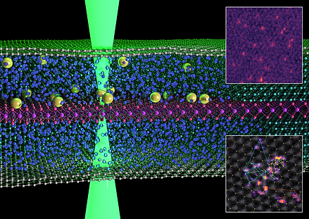
atomic_10_comp_edit_2.png

Cross-section of a double liquid cell structure. Two hBN spacer layers, each tens of nm thick, with a molybdenum disulfide (MoS2) monolayer sandwiched between them (central layer, coloured purple in the figure). Both hBN spacers contain voids pre-patterned using electron-beam lithography and reactive-ion etching. Liquid samples are trapped inside the voids using few-layer graphene (FLG) on the top and bottom of the stack (coloured in green). The atomically flat hBN crystals form a hermetic seal with graphene and MoS2.  Inset top right: HAADF-STEM image. The probe is focused on the submerged MoS2 layer so that the Mo lattice and Pt adatoms are clearly visible . Inset bottom right: A single Pt adatom trajectory from a 134 s video in the graphene double liquid cell

Our engineered graphene liquid cell (EGLC) designs are based on van der Waals heterostructures, with a patterned spacer layer of 2D material defining liquid pockets which are then sealed using graphene. The strong interaction between the 2 atomically flat surfaces generates hermetically sealed individual microwells, with a tuneable thickness down to < 10 nm which is consistent across each cell. The favourable imaging conditions have allowed us to demonstrate nanometre resolution elemental mapping [3], and atomic resolution ADF STEM imaging

TEMFig1.gif

Beam induced growth of dendritic gold particles from solution in Acetone within an EGLC.

Our heterostructure based EGLC also allows for more complicated experiments. For example, by adding a beam sensitive separation layer between two separate EGLC pockets, we can induce local mixing of two precursor solutions directly under the field of view of the microscope by controlled fracturing, allowing us to capture the very earliest stages of solution phase chemical reactions. This was applied to study nonclassical nucleation of calcium carbonate [4] at the nanometre scale.

TEMfig3.gif

Left: Schematic of 2D-mixing cell. Two pockets of separate liquids (represented by red and green spheres) formed in microwells in a hBN flake and sealed with graphene windows are separated by an MoS2 monolayer. The separation layer can be punctured using the beam, allowing the two solutions to mix and react in the direct field of view of the microscope. Right: Nonclassical nucleation of amorphous calcium carbonate from upon mixing 2 precursors. Dense liquid phases formed upon initial mixing spontaneously dehydrate and coalesce to form spherical particles.

[1]    Williamson, M. J., Tromp, R. M., Vereecken, P. M., Hull, R. & Ross, F. M. Dynamic microscopy of nanoscale cluster growth at the solid–liquid interface. Nat. Mater. 2, 532 (2003).

[2]    Yuk, J. M. et al. High-Resolution EM of Colloidal Nanocrystal Growth Using Graphene Liquid Cells. Science 336, 61-64 (2012).

[3]    Kelly, D. J. et al. Nanometer Resolution Elemental Mapping in Graphene-Based TEM Liquid Cells. Nano Lett. 18, 1168 (2018).

[4]    Kelly, D. et al. In situ TEM imaging of solution-phase chemical reactions using 2D-heterostructure mixing cells. Adv. Mater. 33, 2100668 (2021).

​

​

​​

bottom of page